Want to know more?
Don't miss any product updates on our industrial borescopes

Industrial borescope
solution service provider
Company Address
Office : 18F, Pingshanshouzuo, Pingshan District, Shenzhen,Guangdong
Contact Info
Ph: +86-0755-89588241

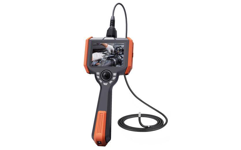
The application of industrial endoscopes in the field of electronic manufacturing is deepening with the growth of precision manufacturing and intelligent testing needs. With its technical advantages such as non-destructive testing, high-definition imaging, and flexible operation, it has become a key tool to ensure the quality and reliability of electronic products.The following is a detailed analysis of specific application scenarios, technical characteristics, typical cases, and development trends:

Internal inspection of precision components
Circuit board defect screening: Industrial endoscopes can penetrate circuit board packages to detect internal line connections and component welding quality (such as false solder joints, cold solder joints, and short circuits), avoiding the blind spots of traditional visual inspections. For example, in the production of 5G communication modules, endoscopes can detect 0.1mm solder joint cracks to ensure signal transmission stability.
Semiconductor packaging verification: In the chip packaging process, endoscopes are used to detect wire bonding quality, air tightness, and foreign matter residue. A semiconductor manufacturer reduced the packaging defect rate by 30% through endoscope inspection.
Observation of tiny structures and hidden spaces
Inspection of connectors and sockets: The arrangement and contact status of the pins inside the electronic connector can be clearly observed through an endoscope to ensure high-reliability connection. For example, in the detection of high-voltage connectors for new energy vehicles, the endoscope can detect poor contact caused by pin offset.
Calibration of micro sensors: Detect the layout and sealing of sensitive components inside MEMS sensors to ensure the accuracy of sensors in extreme environments. A medical device company reduced the sensor failure rate by 40% through endoscope detection.
Verification of device housing and package integrity
Waterproof and dustproof level test: The endoscope can penetrate the gap of the device housing, observe the internal sealing structure, and verify the IP67/IP68 protection level. For example, in the waterproof detection of smartphones, the endoscope can detect the lack of sealant in the microphone hole.
Battery pack safety detection: Detect the arrangement of battery cells, welding quality and diaphragm integrity to avoid the risk of thermal runaway. A power battery manufacturer reduced the short-circuit failure rate of battery cells by 50% through endoscope detection.
Ultra-high-definition imaging and quantitative analysis
Resolution breakthrough: 4K/8K CMOS sensor, with laser diode light source, can capture 0.01mm level micro defects.
Three-dimensional measurement function: Single objective lens phase scanning technology realizes accurate measurement of crack length, depth and profile morphology, with an error of ≤0.005mm.
Flexible probe and extreme environment adaptation
Miniaturized design: The probe diameter can be as small as 2.2mm, suitable for detection in small spaces.
Resistant to extreme environments: Some models can work in an environment of -40℃ to 150℃, withstand vibration acceleration, and are suitable for high-temperature scenes such as SMT patch furnaces.
AI defect recognition: Integrated deep learning algorithm, automatic marking of defects such as cracks and foreign objects, and improved detection efficiency.
5G remote monitoring: Supports real-time 4K video transmission to the cloud, and experts can remotely guide on-site inspections, especially for cross-border supply chain quality control.

Circuit board inspection project of a consumer electronics giant
Requirement: Detect the welding quality of BGA chips on high-end mobile phone motherboards, requiring the detection of 0.05mm microcracks.
Solution: Select the K series endoscope of Microvision Optoelectronics.
Results: Improved inspection efficiency, reduced defective product outflow rate, and annual cost savings for a single production line.
Case: Through endoscope inspection, a batch of battery module cell tabs were found to have poor welding, and the problem batches were isolated in time to avoid the risk of thermal runaway.
Data: The inspection time was shortened and the defect detection rate was improved.
Technology integration and innovation
Multimodal inspection: Integrate infrared thermal imaging, ultrasonic inspection and other functions to achieve "one mirror for multiple uses".
Breakthrough in materials science: Develop radiation-resistant and explosion-proof endoscopes to meet the needs of high-barrier industries such as aerospace.
Industry customization and ecological construction
Vertical field solutions: Develop special inspection software and databases for industries such as semiconductors and new energy vehicles.
Data service extension: From equipment sales to "testing services + data analysis", providing equipment health management (PHM) solutions.
Green manufacturing and sustainable development
Environmentally friendly material application: Use degradable probe materials and low-power circuit design to reduce carbon emissions.
Circular economy model: Launch probe rental services to reduce corporate testing costs.
Industrial endoscopes have become explorers of the "microcosm" in the field of electronic manufacturing, and their technological evolution is driving the industry towards "zero defect" manufacturing. With the deep integration of technologies such as AI and 5G, endoscopes will be more deeply integrated into the intelligent manufacturing system in the future, building a stronger line of defense for the quality and safety of electronic products.

Industrial borescope
solution service provider